|
HOME
ESR
EXPERIMENTS
LABS etc
|
|
E121
E127
E132
E125
E143
laser_cooling_2021
E142
Ę128
E146
E0052
E0018
E0028
E0038
E0075
E0203_E0018
E0052_2025
E0281 - NEEC
|
| Bound beta decay experiment on Tl-205 |
Not logged in |
 |
|
|
|
Message ID: 3
Entry time: Wed Dec 5 17:29:24 2018
|
| Author: |
Chen, Sidhu |
| Category: |
Detectors |
| Subject: |
signal map |
|
|
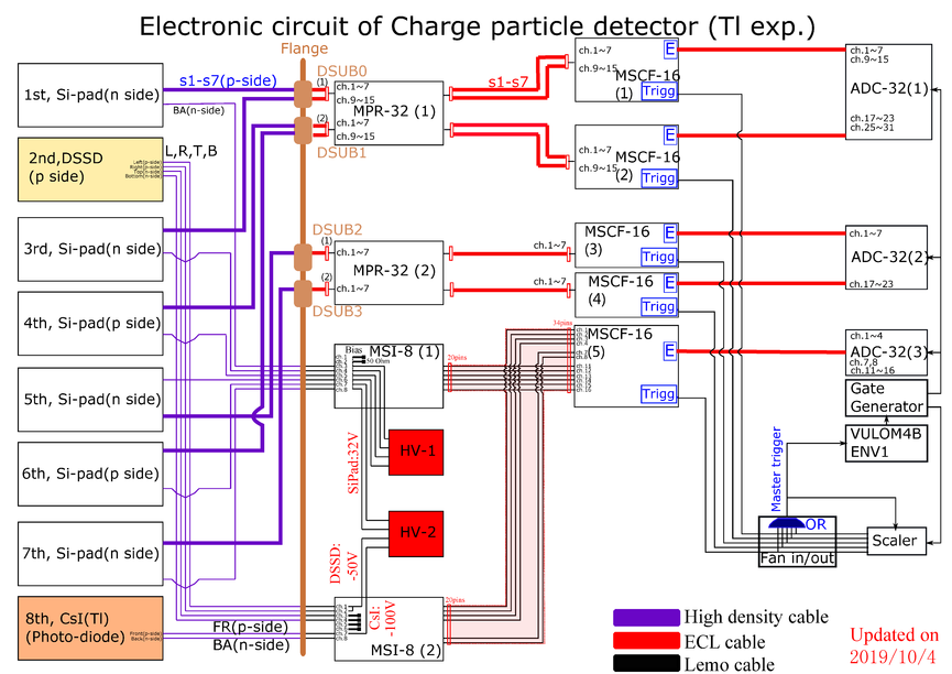
Description:
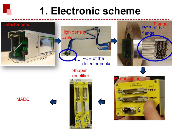
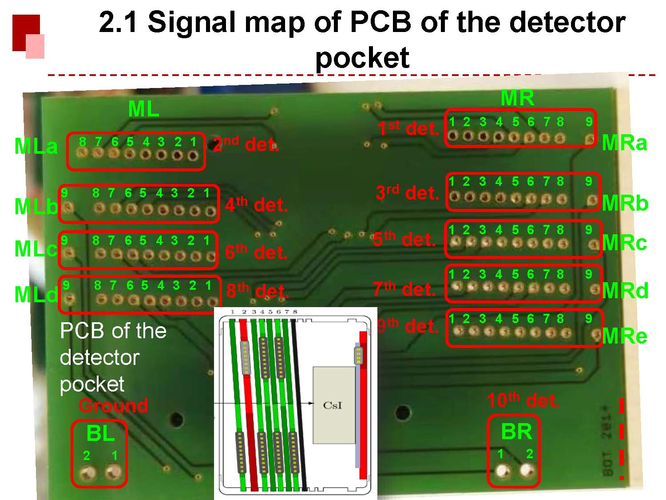
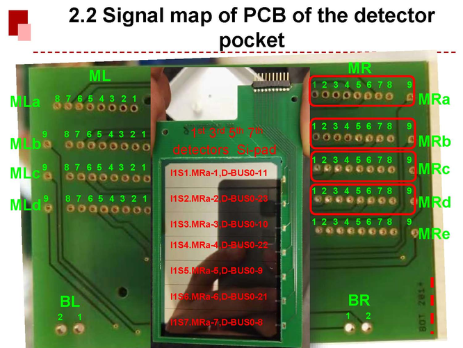
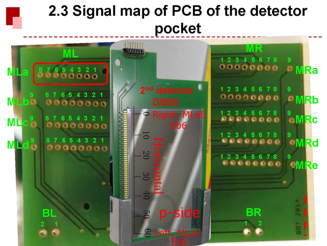
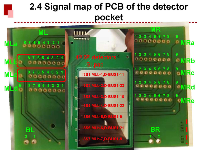
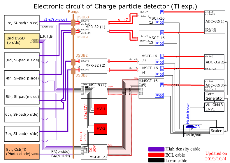
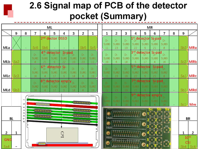
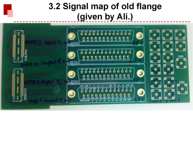
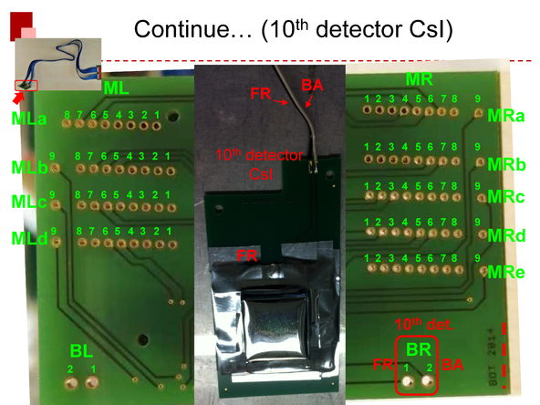
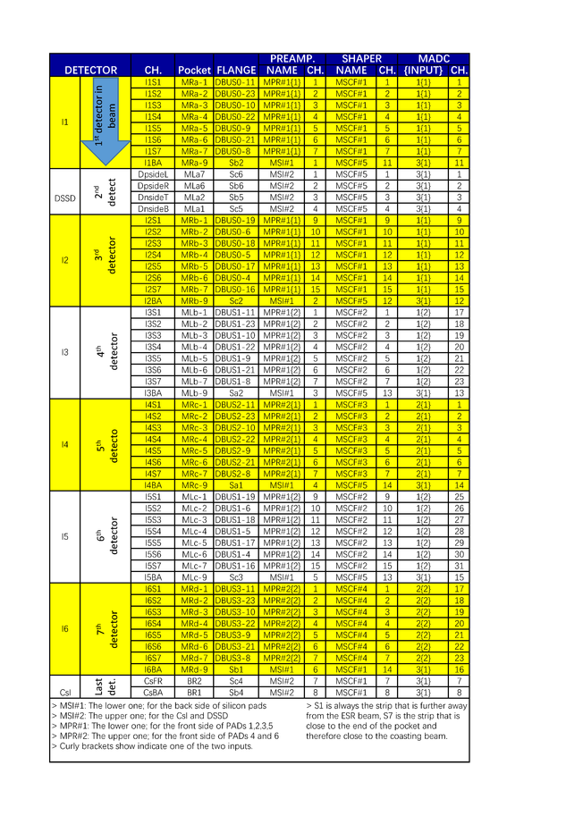
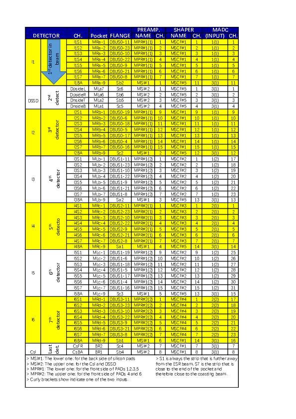
Here is a summary of signal map. The charged particle detector includes 6 layers of Si-Pad, 1 DSSD and 1 CsI.
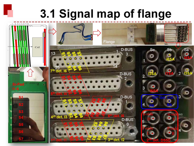
All these detectors are installed inside the detector pocket. All signals are connected to one PCB which is attached on the pocket, then are connected
to the PCB of the flange by high density cable. This document descripts the signal map on the PCB of the detector
pocket and flange.
The signal maps of the PCB of the detector pocket are shown as follow:
 |